The Johnson® Patented High Frequency End Launch connectors are used to transition microwave energy from coaxial to planar transmission line structures. These patented connectors provide a unique solution for microwave engineers who fabricate circuit designs on very thin high frequency board substrates. The in-line connector design minimizes reflections in comparison to a right-angle, perpendicular, PC mount transition.
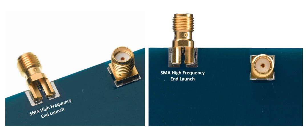
Figure 1: In-Line Connector Design vs Right-Angle, Perpendicular, PC Mount Transition.
High Frequency SMA End Launch Connectors for Microwave PC Board Substrates
The Johnson® High Frequency End Launch connector is designed to attach directly to a high frequency coplanar waveguide (CPW) circuit board transmission line, although other lines such as microstrip can be used with good results. These connectors can be used on high frequency PC board substrate layers as thin as 8 mils and operate at frequencies up to 26.5 GHz (see Return Loss chart). These properties make them ideal for applications such as remote sensing and metering, high speed routers and switches, global positioning satellites, phased array antennas, and cellular linear power amplifiers.

Figure 2: Coaxial vs Coplanar Transmission Line Structures.
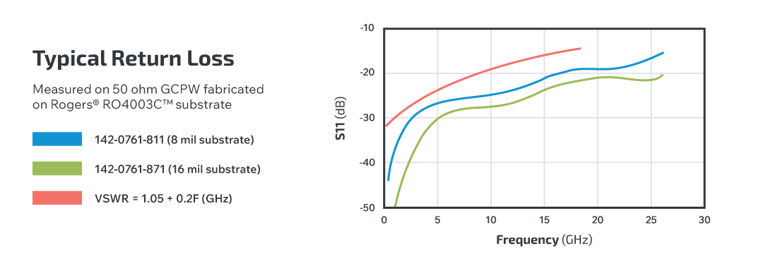
Figure 3: Typical Return Loss for Johnson® High Frequency End Launch Connectors.
Design Features
This connector is an economical alternative to other high frequency designs in the industry. This patented design differentiates itself from other launch connectors:
- Design of the connector is self contained, no external mounting screws, adapter sections, spring clips, etc. are required for assembly to the circuit board.
- Center contact pin does not require special orientation to the surface of the circuit board. The center contact is mechanically captivated and optimized to maintain proper impedance while withstanding torque and axial force stress.
- Output coax of the connector at board launch is sized appropriately to match the thickness of the high frequency board substrate. The output coax section extends well within the connector while maintaining constant inner and outer coaxial diameters.
- Signal side grounding legs of the connector are spaced close enough to keep grounding paths short, but far enough apart to maintain constant impedance in the launch transition area.
- Signal side grounding legs and GCPW geometry control radiation, no additional shielding is required to prevent signal cross-talk effects in the transition area. The launch transition is effectively isolated from adjacent transmission lines in the signal plane.
- Connector is not locked into position when placed on the circuit board. Intentional floating design allows proper alignment in X, Y and Z, minimizing discontinuities due to manufacturing tolerances.
- The new distinctive through hole mounting technique allows the use of one connector with varying circuit board thicknesses. The connectors are also available in a traditional straddle mount end launch design, which was pioneered by Johnson - Cinch Connectivity Solutions over 20 years ago.
- A small amount of PTFE insulation projects from the rear mating plane of the connector, acting as a seal when soldering the center conductor pin to the trace. The connector is held against the circuit board edge during the soldering process, compressing the PTFE insulation. This effectively creates a barrier between the inner and outer conductors, preventing the bridging of solder.
- Appropriate sized connectors do not require additional compensation to standard coplanar or microstrip matched impedance line geometries. Transition can be fine-tuned by pulling the trace back a slight amount from the board edge.
Mounting Instructions for SMA High Frequency End Launch Connectors
Mounting Footprint Info
- All of the drilled holes are plated through the entire circuit board stackup.
- All hole patterns are symmetrical about center of the trace.
- The recommended mounting footprints are shown for the top (signal) side of the board only. Use ground planes on additional layers where appropriate.
- For optimum high frequency circuit board performance, use the following fabrication guidelines:
- Maintain a solid ground plane below the high frequency substrate layer
- Control the pullback of the trace and grounds from the board edge
- Continue the grounded coplanar waveguide line beyond the ground pad area.
- Place 16 mil diameter ground vias on both sides of the coplanar waveguide line, spaced at 50 mil intervals along the entire length of the line.
- Immersion gold plate (ENIG) all high frequency conductors per IPC-4552.
- Do not coat the coplanar waveguide signal trace or open ground gaps with soldermask.
| GCPW 50Ω Impedance Reference Dimensions * | Mounting and Via Holes | ||||||
|---|---|---|---|---|---|---|---|
| Part Number | Substrate Thickness | Conductor Thickness | Trace Width "A" | Fig | "C" | "D" | |
| 142-0761-801 | .0080 (0.203) | .0014 (0.036) | .0155 (0.394) | 1 | .066 (1.68) | .096 (2.44) | |
| 142-0761-811 | .0080 (0.203) | .0014 (0.036) | .0155 (0.394) | 1 | .066 (1.68) | .096 (2.44) | |
| 142-0761-821 | .0160 (0.406) | .0014 (0.036) | .0285 (0.724) | 1 | .084 (2.13) | .113 (2.87) | |
| 142-0761-831 | .0160 (0.406) | .0014 (0.036) | .0285 (0.724) | 1 | .084 (2.13) | .113 (2.87) | |
| 142-0761-841 | .0080 (0.203) | .0014 (0.036) | .0155 (0.394) | 2 | .066 (1.68) | ||
| 142-0761-851 | .0080 (0.203) | .0014 (0.036) | .0155 (0.394) | 2 | .066 (1.68) | ||
| 142-0761-861 | .0160 (0.406) | .0014 (0.036) | .0285 (0.724) | 2 | .084 (2.13) | ||
| 142-0761-871 | .0160 (0.406) | .0014 (0.036) | .0285 (0.724) | 2 | .084 (2.13) | ||
| 142-0761-881 | .0080 (0.203) | .0014 (0.036) | .0155 (0.394) | 1 | .066 (1.68) | .096 (2.44) | |
| 142-0761-891 | .0080 (0.203) | .0014 (0.036) | .0155 (0.394) | 2 | .066 (1.68) | ||
| 142-0761-821 | .0160 (0.406) | .0014 (0.036) | .0285 (0.724) | 1 | .084 (2.13) | .113 (2.87) | |
| 142-0761-831 | .0160 (0.406) | .0014 (0.036) | .0285 (0.724) | 2 | .084 (2.13) | ||
Figure 4: Reference Dimensions for 50 ohm Grounded Coplanar Waveguide using Rogers Corporation RO4003C™ High Frequency Substrate Laminate*.
*These calculated dimensions assume a quasi-tatic mode of propagation, but dispersion does exist for coplanar waveguide. The characteristic impedance and effective dielectric constant may increase slightly for X-band and higher frequencies, unless very small ground to ground gap spacing is used.
It is assumed the conductors have rectangular cross-sections. The etching process used in circuit board fabrication actually produces trapezoidal shapes. Therefore, the GCPW impedance may increase somewhere between that of a perfect rectangular conductor and a theoretical zero thickness conductor.
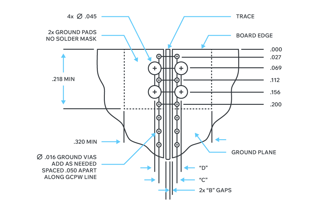
Figure 5: Recommended PCB layout top.
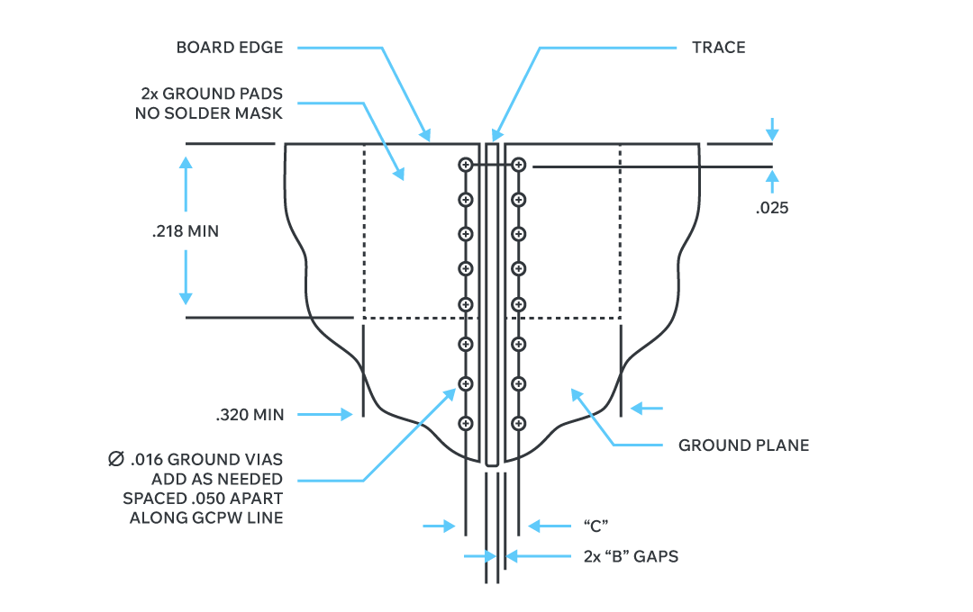
Figure 6: Recommended PCB layout bottom.
PC Mounting Instructions
High frequency end launch performance is dependent upon proper mounting. The following factors must be controlled for optimum performance:
- The connector should fit tightly against the circuit board edge, avoid gaps.
- The center contact pin must lie parallel and flat against the circuit board, avoid gaps.
- The contact pin should be centered on the circuit board signal trace.
- Use a minimal amount of solder between the contact pin and signal trace. Do not allow excess solder to build up or flow down the trace.
- Clean all excess flux and other residue from the launch area, especially between the trace and ground
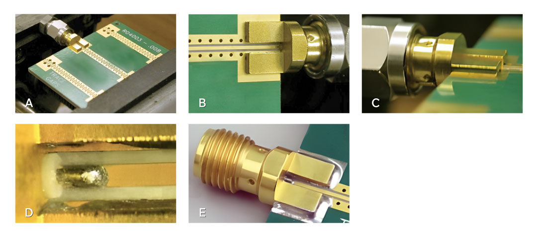
Figure 7: Mounting a High Frequency End Launch Connector: Step by Step.
The basic steps required to mount the end launch connector to the circuit board are as follows:
- Fixture 140-0000-973 should be used as an aid during manual soldering. The fixture protects the connector from damage during clamping and also maintains the proper location of the connector’s insulator and contact. To use the fixture, thread the coupling nut on the mating end of the connector and hand tighten. This mounting assembly can now be held in a vice or similar clamping device.
- Position connector on the circuit board, making sure the contact pin is aligned with the center of the signal trace. Make sure that the connector legs and contact pin are held flush against the top of the circuit board, keeping the axis of the connector parallel to the plane of the circuit board.
- A small amount of Teflon® insulation projects from rear mating plane of the connector, which acts as a seal when soldering the center conductor pin to the trace. Clamp the connector ightly against the edge of the board. This action compresses the insulator seal against the board edge. This effectively creates a barrier between the inner and outer conductors preventing the bridging of solder.
- While ensuring the connector is held in the correct position, solder the ground legs and/or ground posts to the top and bottom of the board prior to bonding the center pin to the trace.
- Once the connector body is properly grounded to the board, the center contact pin can be bonded to the trace by using a minimal amount of solder. It is important that solder flows along the length of the exposed pin, creating a good electrical and mechanical connection. Remove any excess solder that is not required for a solid joint.
- Clean all flux and other residues from the trace area between the signal side ground legs, as any flux present between the signal trace and ground will affect performance. The completed mounting assembly should look similar to the one shown in the image above.
Grounded Coplanar Wave Guide Design Guideline for SMA High Frequency Connectors
Easily Connected to GPCW Transmission Lines with Reproducible Results
A coplanar waveguide transmission line is formed by a planar conductor separated by a pair of ground planes, all on the same plane, atop of a high frequency dielectric medium. A variant is formed when a ground plane is provided on the opposite side of the dielectric which is called grounded coplanar waveguide (GCPW). Although GCPW is the preferred transmission line structure on the circuit board for this connector, other lines such as microstrip can be used with good results.
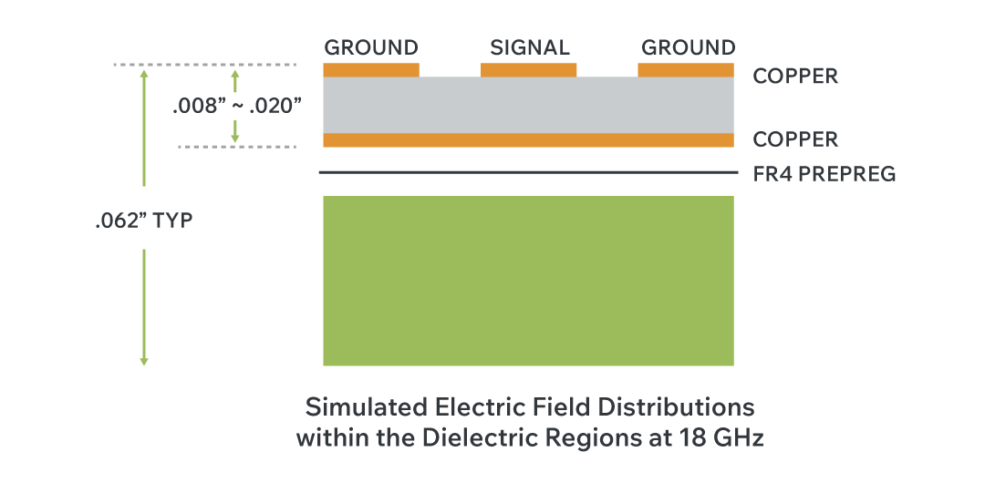
Figure 8: Simulated Electric Field Distributions within the Dielectric Regions at 18 GHz.
At microwave frequencies, the coplanar waveguide can be equal to or better than the microstrip when loss and dispersion are used as a basis for comparison. Minimum loss for a given coplanar waveguide occurs at about 60 Ohms whereas the minimum loss for microstrip occurs at about 25 Ohms. A full wave analysis which includes space wave and surface wave radiation shows that coplanar waveguide discontinuities radiate much less energy than microstrip discontinuities.
The GCPW transmission line is fabricated on a high frequency circuit board substrate. Dielectric constant control, low dissipation factor and controlled thicknesses differentiate these high frequency circuit board materials from those typically used in the high volume printed circuit board world like FR4 and BT/epoxy. For higher frequencies, dielectric loss becomes an important contributor to the total loss. This is important because, as the frequency increases, the thickness of the material must decrease in order to avoid generating transverse modes on the transmission lines.
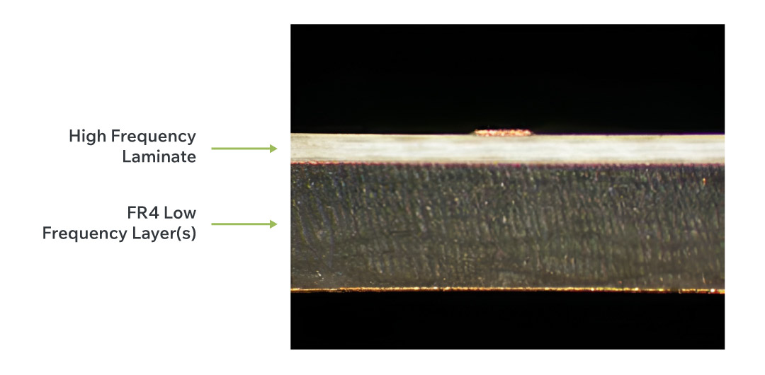
Figure 9: Hybrid Circuit Board Construction.
The high frequency material’s low loss performance extends the useful range of these materials well above 20 GHz. However, very thin dielectric layers as small as .008” are not mechanically stable enough to support the connector and associated circuitry. Therefore, hybrid circuit board constructions consisting of high frequency laminates and epoxy/glass substrates have become an increasingly utilized alternative to lower overall circuit board costs. The DC, control and digital signal paths are designed onto the lower cost epoxy/glass FR4 layer and the microwave signals are carried on the high frequency top layer as shown in Figures 1A and 1B.
As can be seen in the cut away portion of Figure 1, the connector’s center conductor pin is directly attached in-line with the GCPW signal trace. The body of the connector is always attached to the signal side ground. The design of the center conductor pin is a compromise between ease of assembly and minimal discontinuity reactance. The diameter of the pin is matched approximately to the thickness of the GCPW structure. Scaling down the pin diameter matches the electromagnetic field distributions with the GCPW line in order to keep the discontinuity reactance small.
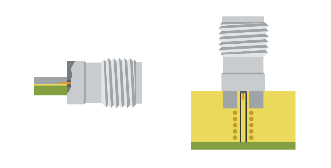
Figure 10: End Launch Connector Shown Attached to the GCPW Transmission Line.
The output coax of the connector at the transition area is sized appropriately to match the thickness of the high frequency board substrate. The output coax section extends well within the connector by means of constant diameters, avoiding any abrupt diametrical changes at the circuit board edge which can create large discontinuities.
Low VSWR and Insertion Loss Over a Wide Bandwidth
An accurate characterization of packaged microwave circuits, such as broadband MMIC power amplifiers, requires coaxial to planar transitions with low return and insertion loss. In order to achieve low loss, the transition design between the launch connector and the printed circuit board requires the optimization of both mechanical and electrical features. The mechanical design must physically match the electromagnetic field distribution as close as possible in order to keep the discontinuity reactances small, as shown in Figure 1. The electrical design must match the impedances and other interface discontinuity reactances over the entire bandwidth.
Minimizing the discontinuity reactances is desired rather than just compensating for them. Compensation can limit the usable frequency range of the connector, if the reactances are too large. The connector design incorporates an internal matched impedance transition from a large input coaxial connector interface, such as SMA, to a small coaxial output matched to the size of the PC board high frequency substrate. The internal transition between the input and output consists of graduated coaxial diametrical step sections, each optimized in size with inductive offsets to reduce the capacitive discontinuities created by the change in coaxial diameters. As shown in Figure 1, using multiple coaxial step sections to match the size of the circuit board reduces the overall effect of the discontinuities, thereby increasin the usable frequency range of the launch connector.
The transition between the launch and the PC board is designed for attachment to grounded coplanar waveguide (GCPW) transmission lines. The signal output pin of the launcher is optimized in both length and diameter to match the corresponding GCPW line. The geometrical size of the signal side ground leg pairs is optimized in height, length and center to center spacing to match the output pin and GCPW line. The combination of optimal signal pin and ground leg design minimizes the attachment discontinuity reactance.
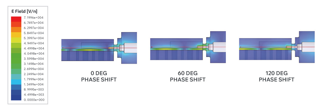
Figure 11: Simulated Electric Field Distributions within the Dielectric Regions at 18 GHz.
Explore Cinch's full range of High Frequency End Launch Connectors

 Johnson High Frequency Connectors