Product Overview
It takes more than an ordinary connector to support advanced performance interconnect applications. CIN::APSE® is a proven solderless Z-axis connector technology that offers exceptional mechanical and electrical performance at signals well above 50GHz.
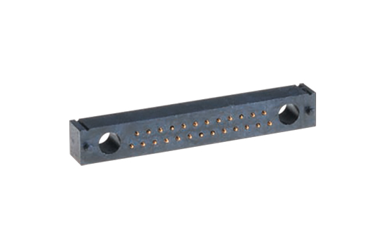
Stacking Connectors
Stacking connectors for connecting PCB or flex, PCB to PCB or component to PCB without the use of solder.
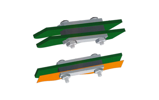
Stacking Connector Hardware
Hardware that has been designed to maintain uniform compressive force across all contacts.
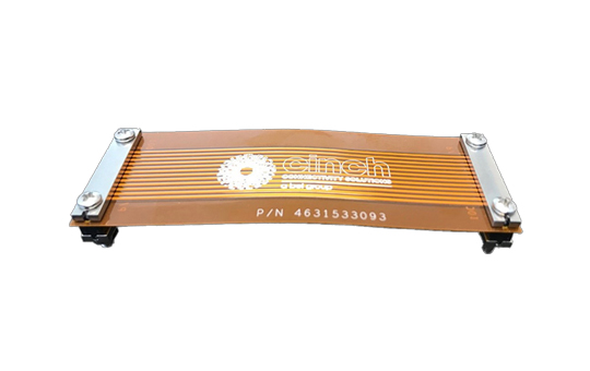
Stacking Connector Jumpers and Assemblies
Short flex PCB assemblies for coplanar and right angle board-board connections.
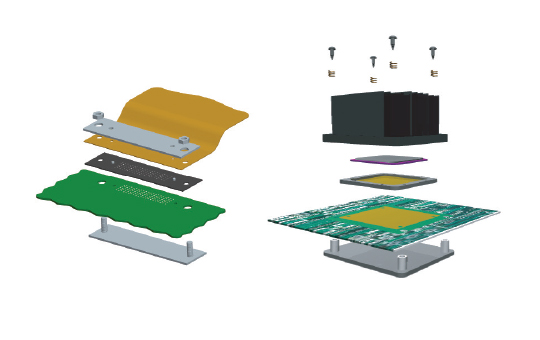
How CIN::APSE® Works
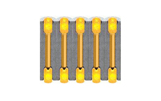
Connection
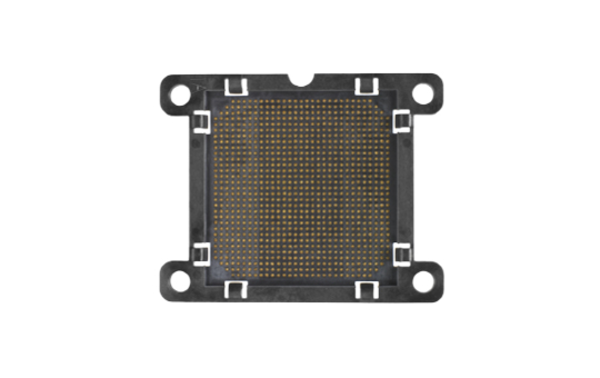
The connectors are constructed by two main components, insulating housing and an electrically conducting contact. The liquid crystal polymer insulators are molded and the contacts are a bundled gold-plated molybdenum wire. Gold plated copper spacers are used for long Z-axis connectors.
Positioning
The positioning is designed into the insulating housing. Insulation housing are molded for high volume and machined for prototypes.
Mounting
The connectors are positioned and mounted between boards and components using generally available alignment and compression hardware. Hardware can be press fit into PCB or utilized with a bolster plate for maintaining even compression across a large socket. Designers recommend PCB layout for gold plated pads and alignment holes locations.
Key Features
Stacking Connectors
- Maximize SWaP (Size, Weight, and Performance) for space and weight constrained designs
- Pitch grid of 2.00 mm, 1.0 mm and 0.80 mm achievable
- Thin profiles from 0.020" and greater
- 2-piece design reduces additional space and weight
Solderless
- Compression sufficient for establishes multiple points of contact, RoHS compatible
- No thermal processing or X-ray inspection required
- Reversible mating process for multiple cycles
Customizable
- Design team available for mechanical drawings and product sketches
- Prototypes available for low quantities
- Profile thicknesses from 0.020" to 1.0"
- 2 to 7,356 contacts have been used per connector, but no limit exists
- IC-to-PCB, PCB-to-PCB, Flex-to-PCB, Component-to-PCB
Reliable
- Excellent shock and vibration stability, 100 Gs shock, 20 Gs vibration
- Thermally stable, life and cycle testing, 5,000 hrs @ 170°C
- Electrically stable, > 1,000 MΩ @ 500 VDC
Applications
The CIN::APSE solderless compression connector technology is the most widely implemented crimpless and solderless high speed interconnect system for key industries including Commercial Aerospace, Space, Defense, Test & Measurement. Examples of the applications include:
Geostationary Communication Platforms
Inertial Navigation Systems
Network Switches
Digital Surveillance Systems
CPU and ASIC-to-board Connections
Discover CIN::APSE®
Discover why CIN::APSE® is the most widely implemented crimpless and solderless, high speed interconnect in the industry.
Let’s Discuss What’s Possible